NOTES for PCB DESIGN SETTING
1. Trace
To designer, we can’t only consider the precision and perfect requirements of the design, the major constrain is the manufacture technology. It’s possible that the product made out is different from the original version design.
The manufacturer won’t build a new production line just for a good design. We need to learn from the experience, we have to design the best product under the current manufacture conditions. Including the basic spec like quantity of PCB layer, board thickness, via diameter, the min trace and space, copper thickness etc. And the special requirement like board material, surface plating, and other specific requirement. Normally the PCB orders are divided into prototype order and finial production order. To designator, it’s the finial production order that has practical significance. So we need to strictly observe the technological requirements of production order.
To the technology requirement about product precision, the min trace and space, and the min via diameter are the most major and most important specs. Which shows the manufacturer can deal with how narrow trace and how small via. If the trace width in your design is smaller than the min trace spec, then it’s too narrow to be made out. The trace and space precision will also impact whether the words and patterns in the silkscreen are clear. If the via diameter in your design is too small, then there won’t be a suitable drill can support.The min drill size can also impact the mechanical hole, mounting hole and the precision of outline sloting in any way.
In PCB design, for example if the min trace and space for production order is 4mil, means the trace width in the design has to be more than 4mil, and the space between trace also has to be more than 4mil. This is just to define the min trace and space, in actual design, the traces need to be of different width. For example, the power network trace should be wider than the signal trace.
These different requirement can be defined in rule, define different trace width values in different nets, then WHERE set the priority of rule applications basing on the importance degree. It’s same to the trace space, you can define the electrical safety space between different nets in the rule page Design - Rules - Electrical – Clearance.
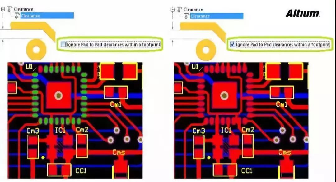
There’s a special situation. To high-density pin component, the clearance between pads will be very narrow, such as 6mil. Even if it satisfies the technological requirement of min trace and space, it may can’t meet the design rule.
If the set of whole PCB’s min safety clearance is 8mil, then it’s apparently the clearance of component’s pads break the rule setting. Violations will always be highlighted in green during rule checking or online editing. But as we know, this violation doesn’t need to be dealt with. Previously, in the old version software, we have to use the Query language to define a different safe spacing rules for this component, and set it to high-priority. Now, in the new version software, we just need to easily check the option ‘Ignore Pad to Pad clearance within a footprint’, like below pic. It’s much more convenient than before.

2. Via
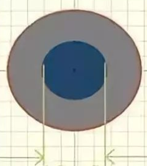
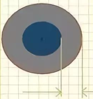
Normally the min via diameter is 6mil, the min via ring is 8mil, the clearance between vias is 6mil.
 6mil
6mil
 8mil
8mil
 6mil
6mil
The min via diameter and min clearance between vias are very important content in design rule. We have to pay much attention on.
3. Pad
1) The plug-in via size depends on the component. The via has to be larger than the component’s pin. The advice is the via should be at least 0.2mm larger than componet’s pin. For example, the via for a 0.6mm pin should be at least 0.8mm. It’s to avoid the component can’t be plugged into the via since manufacture tolerance.
2) Regarding the via ring of PTH and the clearance between PTHs, larger is better.
3) The clearance between pad and board edge should be at least 0.3mm to individual boards, and not less than 0.35mm to boards in V-cut panel.
4. Solder Mask
The SMD solder mask opening can’t be less than 0.1mm(4mil) on one side.
5. Silkscreen
The width of silkscreen can’t be less than 6mil.
Capacités
Capacité PCB rigide
Capacité PCB flexible
Capacité d'assemblage PCB
Équipement PCB
Équipement d'assemblage PCB
Méthodes de paiement
Prix spéciaux
Transporteurs
Support pour amateurs
Certificat
Assistance clientèle
Suivez-nous
Tel: 1-905-339-2881
Email: [email protected] , [email protected]
Copyright Gold Phoenix PCB Co., Ltd. 2011 - 2023
Tel: 1-905-339-2881 Email: [email protected] , [email protected]
Système de contrôle qualité | Service produit
| Liens
Copyright Gold Phoenix PCB Co., Ltd. 2011 - 2023


