Ball Grid Array
Description

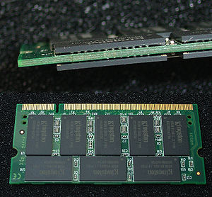
BGA ICs assembled on a RAM stick
The BGA is descended from the pin grid array (PGA), which is a package with one face covered (or partly covered) with pins in a grid pattern which, in operation, conduct electrical signals between the integrated circuit and the printed circuit board (PCB) on which it is placed. In a BGA the pins are replaced by pads on the bottom of the package, each initially with a tiny solder ball stuck to it. These solder spheres can be placed manually or by automated equipment, and are held in place with a tacky flux. The device is placed on a PCB with copper pads in a pattern that matches the solder balls. The assembly is then heated, either in a reflow oven or by an infrared heater, melting the balls. Surface tension causes the molten solder to hold the package in alignment with the circuit board, at the correct separation distance, while the solder cools and solidifies, forming soldered connections between the device and the PCB.
In more advanced technologies, solder balls may be used on both the PCB and the package. Also, in stacked multi-chip modules, solder balls are used to connect two packages.
Advantages
High density
The BGA is a solution to the problem of producing a miniature package for an integrated circuit with many hundreds of pins. Pin grid arrays and dual-in-line surface mount (SOIC) packages were being produced with more and more pins, and with decreasing spacing between the pins, but this was causing difficulties for the soldering process. As package pins got closer together, the danger of accidentally bridging adjacent pins with solder grew.
Heat conduction
A further advantage of BGA packages over packages with discrete leads (i.e. packages with legs) is the lower thermal resistance between the package and the PCB. This allows heat generated by the integrated circuit inside the package to flow more easily to the PCB, preventing the chip from overheating.
Low-inductance leads
The shorter an electrical conductor, the lower its unwanted inductance, a property which causes unwanted distortion of signals in high-speed electronic circuits. BGAs, with their very short distance between the package and the PCB, have low lead inductances, giving them superior electrical performance to pinned devices.
Disadvantages

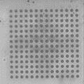
X-ray of BGA
Noncompliant connections
A disadvantage of BGAs is that the solder balls cannot flex in the way that longer leads can, so they are not mechanically compliant. As with all surface mount devices, bending due to a difference in coefficient of thermal expansion between PCB substrate and BGA (thermal stress) or flexing and vibration (mechanical stress) can cause the solder joints to fracture.
Thermal expansion issues can be overcome by matching the mechanical and thermal characteristics of the PCB to those of the package. Typically, plastic BGA devices more closely match PCB thermal characteristics than ceramic devices.
The predominant use of RoHS compliant lead-free solder alloy assemblies has presented some further challenges to BGAs including "head in pillow" soldering phenomenon, "pad cratering" problems as well as their decreased reliability versus lead-based solder BGAs in extreme operating conditions such as high temperature, high thermal shock and high gravitational force environments, in part due to lower ductility of RoHS-compliant solders.
Mechanical stress issues can be overcome by bonding the devices to the board through a process called "underfilling", which injects an epoxy mixture under the device after it is soldered to the PCB, effectively gluing the BGA device to the PCB. There are several types of underfill materials in use with differing properties relative to workability and thermal transfer. An additional advantage of underfill is that it limits tin whisker growth.
Another solution to non-compliant connections is to put a "compliant layer" in the package that allows the balls to physically move in relation to the package. This technique has become standard for packaging DRAMs in BGA packages.
Other techniques for increasing the board-level reliability of packages include use of low-expansion PCBs for ceramic BGA (CBGA) packages, interposers between the package and PCB, and re-packaging a device.
Difficulty of inspection
Once the package is soldered into place, it is difficult to find soldering faults. X-ray machines, industrial CT scanning machines,special microscopes, and endoscopes to look underneath the soldered package have been developed to overcome this problem. If a BGA is found to be badly soldered, it can be removed in a rework station, which is a jig fitted with infrared lamp (or hot air), a thermocouple and a vacuum device for lifting the package. The BGA can be replaced with a new one, or it can be refurbished (or reballed) and re-installed on the circuit board. Pre-configured solder balls matching the array pattern can be used to reball BGAs when only one or a few need to be reworked.
Due to the cost of visual X-ray BGA inspection, electrical testing is very often used instead. Very common is boundary scan testing using an IEEE 1149.1 JTAG port.
A cheaper and easier inspection method, albeit destructive, is becoming increasingly popular because it does not require special equipment. Commonly referred to as dye and pry, the process includes immersing the entire PCB or just the BGA attached module into a dye, and after drying, the module is pried off and the broken joins are inspected. If a solder location contains the dye, then it indicates that the connection was imperfect.
Difficulties during circuit development
During development it is not practical to solder BGAs into place, and sockets are used instead, but tend to be unreliable. There are two common types of socket: the more reliable type has spring pins that push up under the balls, although it does not allow using BGAs with the balls removed as the spring pins may be too short.
The less reliable type is a ZIF socket, with spring pinchers that grab the balls. This does not work well, especially if the balls are small.
Cost of equipment
Expensive equipment is required to reliably solder BGA packages; hand-soldering BGA packages is very difficult and unreliable, usable only for the smallest packages in the smallest quantities. However, as more ICs have become available only in leadless (e.g. quad-flat no-leads package) or BGA packages, various DIY reflow methods have been developed using inexpensive heat sources such as heat guns, and domestic toaster ovens and electric skillets.
Capacités
Capacité PCB rigide
Capacité PCB flexible
Capacité d'assemblage PCB
Équipement PCB
Équipement d'assemblage PCB
Méthodes de paiement
Prix spéciaux
Transporteurs
Support pour amateurs
Certificat
Assistance clientèle
Suivez-nous
Tel: 1-905-339-2881
Email: [email protected] , [email protected]
Copyright Gold Phoenix PCB Co., Ltd. 2011 - 2023
Tel: 1-905-339-2881 Email: [email protected] , [email protected]
Système de contrôle qualité | Service produit
| Liens
Copyright Gold Phoenix PCB Co., Ltd. 2011 - 2023


